
Ads by Google
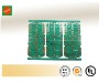

multilayer pcb board manufacture
1.Model:2-layer
2.Material: FR-4
3.Copper thickness: 3OZ
4.Board thickness: 1.6mm
5.Finish: Immersion gold
6.Solder mask color: green
7. Min Diameter of Drilling Hole:0.25mm
8.Min Diameter of Punched Hole:0.9mm
9.Tolerance
Position of Drilled Hole: +/- 0.075mmTrace Width: +/- 075mmAperture :PTH±0.075mmWarpage >0.7Specification:
1.Factory Price 2.Certification:UL, ISO9001,SGS,IPC 3.Prompt delivery 4.High quality 5.Good wills with our clients
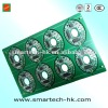
Shenzhen Factory PCB assembly & PCBA assembly OEM service for Electronics Field
Applications: Computer PCBA, network card &communication card /pcb assembly -Small orders can be accepted
- Experienced Technical Staff - Competitive Price - Product Features - Customized Service - Small Order Accepted - Quality Approval
Item | Capalitily | ||
1.Layer | 1-18 | ||
2.Basic Material | CEM-3,FR-4,CEM-1 | ||
3.Board Thickness | 0.2mm-3.2mm (8mil-126mil) | ||
4.Min Thickness of Core Board | 0.1mm(4mil) | ||
5.Copper Thickness | Min:1/3 oz ; Max:3 oz | ||
6.Min Trace Width/Space | 0.075mm(3mil) | ||
7.Min Diameter of Drilling Hole | 0.25mm(10mil) | ||
8.Min Diameter of Punched Hole | 0.9mm(35mil) | ||
9.Tolerance | Position of Drilled Hole | ±0.075mm(3mil | |
Trace Width | ±0.05mm(2mil) | ||
Aperture | PTH±0.075mm(3mil) NPTH±0.05mm(2mil | ||
Outline Tolerance | Drilling: ±0.13mm(6mil) | ||
Warpage | >0.7 | ||
10.Surface Treatment | Gold,Plating/Immersion Gold/HAL/HAL lead-free/Immersion Silver/Entek | ||
1I.nsulation Resistance | 10KΩ-20MΩ | ||
12.Conduction Resistance | < 50Ω | ||
13.Testing Voltage | 300V | ||
14.V-CUT |
| Min:110×100mm Max:660×600mm | |
Board Thickness | Min:0.6mm(24mil) | ||
Reserved Thickness | Min:0.3mm(12mil) | ||
Tolerance | ±0.1mm(4mil) | ||
Slot Width | Max:0.50mm(20mil) | ||
Slot to Slot | Min:10mm | ||
Slot to Trace | Min:0.50mm(20mil) | ||
15.Slot | Slot size:tol.>=2W(tolerance) | PTH L:±0.15mm(6mil) W:±0.1mm(4mil) | |
NPTH L:±0.125mm(5mil) W:±0.1mm(4mil) | |||
16.Min Hole Pad | PTH :0.13mm(5mil) | ||
NPTH :0.18(7mil) | |||
17.Multilayer Board | Psition of hole | 0.075mm(3mil) | |
Deviation between Layers | 4 layers: Max 0.15mm(6mil) | ||
6 layers: Max 0.025mm(6mil) | |||
Min insulation hole pad in inner layer | 0.025mm(10mil) | ||
Min Distance from Board Edge to Inner Roundess | 0.25mm(10mil) | ||
Board Thickness | 6 layers:±0.15mm(6mil) | ||
Characteristic Impedance | 60 Ω±10% | ||
If you interested it, send us Gerber File ,pls.
multilayer pcb board manufacture