

Ads by Google

osp surface treatment pcb Spec. |
| Layer: 1-30 |
| Board finished thickness:0.21mm-7.0mm |
| Material:FR-4,CEM-1,CEM-3,High TG,FRS Halogen free ,Rogers |
| Max finished board size: 23*25 (580mm*900mm) |
| Min. drilled hole size: 0.25mm 0.075mm |
| Min. Line Width:3mil 0.075mm |
| Min. line spacing: 3mil 0.075mm |
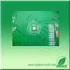
| Surface finish/treatment(finish coattingOO) Hasl/hasl lead free ,Hal, Chemical tin, Chemical gold, immersion silver /gold,OSP,gold plating |
| Copper thickness:35um 1.0oz/3oz-60z |
| Solder mask color: green |
| Board thickness :min0.15mm,Max 7.0mm |
| Copper thickness in hole : 0.5-7.0oz |
| Drilling (min size: mechanical drilling 8mil (0.2mm) laser drilling: 4mil (0.1mm) |
| Inner packing : vacuumized packing inside |
| Outer packing: standard carton packing |
| Shape tolerance: + 0.13 |
| Hole tolerance: PTH: +0.076 NPTH: +0.05 |
| Certificate: UL, ISO9001, ISO 14000, SGS, ROHS, CQC |
| Special req. buried and blind via controlled impendance+BGA |
| Profiling: punching .Routing, v-CUT, Beveling |
| Provides OEM service to all sorts of printed circuit board assembly as well as electronic encased product. |
| Brand name:OEM |
| Solder mask color: green /yellow /black /white /red/blue |
| Lead time: 3-10days |
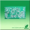
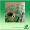
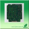
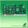
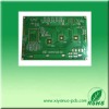
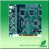
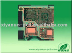
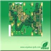
double-sidded osp surface treatment pcb