


Ads by Google
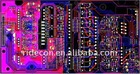

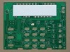
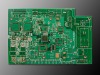
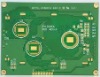
pcb layout design :
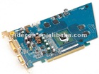
Complete electronic product design from concept to completion: This involves the development of a full fledged, complete "ready to market" product and consists of enclosure design (either based on readily available enclosures, or custom designed mold preparation), hardware design (schematic & PCB design), user interface design (front panel/control panels), firmware/software design, product approvals (CE mark, FCC, UL etc). We are good at converting mere English descriptions into complete products by interacting with clients till we understand what they have in mind.
Layer Count | 1-22 layers HDI |
Material | CEM1,CEM3,FR-4,High TG FR4,halogen-free FR4,aluminium,ceramic etc |
.Maximum Size | 610mm×1200mm |
Board thickness | 0.125mm-6.0mm |
.Minimum Line/Space | 0.075mm |
Minimum Drilling Hole(Mechanical) | 0.15mm |
Minimum Laser Hole | 0.075mm |
Copper Thickness | 17µm-175µm |
Mini Solder Mask Bridge | 0.025mm |
Impedance Control Tolerance | 1.±5% |
Surface finishing | HASL,LEAD-FREE HASL,Immersion gold,Immersion tin,Immersion Silver,Plated gold,OSP,Carbon ink. |
Solder Mask Color | Green,Red,White,Yellow,Black,Blue |
Quality Standards | IPC-A-600F and MIL-STD-105D CHINA GB4588 |
pcb layout design service